Custom sheet metal parts in as little as 3 days - Get a quote now!

What Are Printed Circuit Boards and How Do They Work?

Printed circuit boards are the quiet structure behind modern electronics. They hold components, guide electrical signals, and connect power through carefully designed copper paths. A phone, medical monitor, vehicle controller, and industrial sensor may all depend on them. The term “Printing Circuit Boards” is often used informally, although “printed circuit boards” is the technically accepted expression.

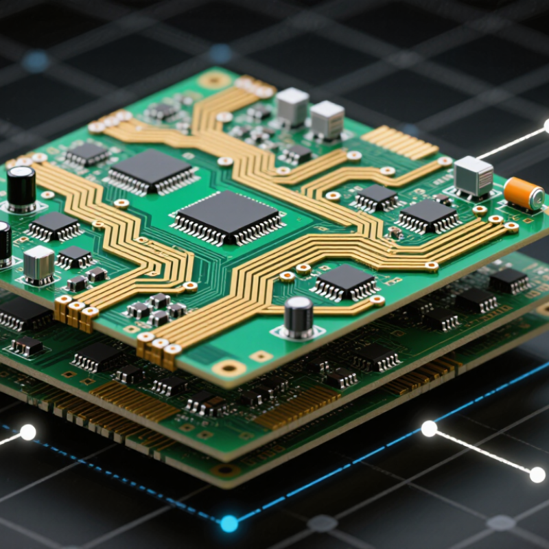
Their operation is easier to understand through a physical example. A multilayer board may contain glass-reinforced material, copper foil, drilled vias, solder mask, and a protective surface finish. Signals travel along copper traces, while vias transfer connections between layers. Components are mounted on the surface and soldered into place. Every width, spacing, and hole must match the design rules. A small defect can create heat, noise, or complete failure.

The industry is expanding with electric vehicles, data centers, renewable-energy systems, and connected devices. Fortune Business Insights estimated the global PCB market at about USD 89.7 billion in 2023, with further growth expected through 2030. IPC’s World PCB Production Report also shows the continuing importance of Asian manufacturing capacity and regional supply chains. These reports offer useful direction, but market forecasts are not guarantees. They can change with material prices, trade policy, and technology shifts. That uncertainty matters. Understanding how a board works requires more than memorizing layers; it requires examining design choices, manufacturing limits, testing methods, and real operating conditions. A board is small. Its responsibilities are not.

What Are Printed Circuit Boards and How Do They Work?

What Is a Printed Circuit Board?

A printed circuit board, or PCB, is a rigid or flexible platform that connects electronic components. It uses copper traces instead of loose wires. These traces carry power and signals across the board. The base material usually combines resin and glass fiber, creating electrical insulation and mechanical strength. Components attach through holes or surface-mounted pads. Tiny vias connect copper layers vertically. In practice, a multilayer PCB can resemble a city map, with highways, intersections, and hidden underground routes. The comparison is imperfect, but useful.

The 2024 Global Printed Circuit Board Market report estimates that the sector could grow from about 83 billion US dollars in 2023 to more than 120 billion dollars by 2030. Industry production data also shows rising demand for high-density interconnect and flexible circuit designs. These figures describe market value, not the number of boards produced, so they need careful interpretation. A PCB does not “think” by itself. It provides controlled paths for current, while processors, memory, sensors, and other components perform specific tasks. During inspection, engineers check trace spacing, solder joints, layer alignment, and impedance. Small defects matter. One damaged via can interrupt an entire signal path. The basic idea seems simple. Manufacturing is not.

The Main Layers and Components of a PCB

What Are Printed Circuit Boards and How Do They Work?

The Main Layers and Components of a PCB

A printed circuit board, or PCB, connects electronic parts through carefully arranged copper pathways. It replaces tangled wires with a flat, structured platform. In a typical board, the substrate provides mechanical support. This layer is rigid and electrically insulating. It often uses a glass-reinforced resin material.

Copper layers carry electrical current between components. A simple PCB may have copper on one side. More complex boards contain several internal copper layers. Thin insulating sheets separate these conductive paths. Small holes, called vias, connect copper routes between layers. Their placement affects signal quality and manufacturing reliability.

The outer surface usually has a protective coating called solder mask. It leaves selected copper areas exposed for soldering. Printed markings identify parts, polarity, and inspection points. These markings are useful during assembly and repair. They can still become unclear on crowded boards.

Key components include resistors, capacitors, diodes, integrated circuits, connectors, and switches. Each performs a specific electrical task. Resistors limit current. Capacitors store charge and reduce unwanted voltage changes. Integrated circuits process signals or control functions. I have found that component spacing matters as much as component choice. Heat, vibration, and electrical noise can change real-world performance. A board may pass a visual inspection yet fail during testing. That is why engineers check traces, solder joints, grounding, and thermal paths repeatedly.

How Electrical Signals Move Through a PCB

A printed circuit board, or PCB, is a layered platform that connects electronic components. Its copper traces guide electrical signals between chips, sensors, connectors, and power sources. A signal begins as a changing voltage or current at one component. It then travels along a carefully shaped copper path. The return current usually follows a nearby ground plane. This path matters. A poor return route can create noise, unwanted radiation, or unstable operation.

Signals do not move like water through an empty pipe. They behave as electromagnetic energy around the trace and its return path. At high speeds, trace width, spacing, copper thickness, and board material affect signal quality. Vias can carry signals between layers, but each via adds a small change in impedance. Sharp corners are often less important than careless routing near gaps in the reference plane. In practical board testing, an oscilloscope may reveal ringing near a connector. That detail can expose a layout problem invisible to the naked eye. The simple model helps, but it is not perfect.

Tips: Keep fast signal traces short and provide a continuous reference plane. Place decoupling capacitors close to power pins. Separate noisy switching paths from sensitive analog routes. Check the return-current path, not only the forward trace. When measurements disagree with simulations, inspect connectors, vias, and probe placement before changing the circuit.

How Printed Circuit Boards Are Designed and Manufactured

Printed circuit boards begin as electrical plans, but manufacturing success depends on disciplined translation. Designers place components, route copper traces, and define a layer stackup in engineering software. They also control trace width, spacing, via size, and impedance. A high-speed board may require controlled 50-ohm paths and carefully separated power layers.

Prismark’s 2024 market data estimated global PCB sales at approximately US$69 billion in 2023. That scale reflects complex production, not simple laminating. Fabricators laminate copper-clad layers, drill thousands of holes, plate the walls, etch unwanted copper, and apply solder masks. Automated optical inspection checks alignment and trace defects. Electrical testing then searches for open or short circuits. IPC design guidance also stresses manufacturability, thermal management, and material selection. A clean schematic can still fail during drilling.

Tips: Leave practical spacing around dense components. Confirm the manufacturer’s minimum drill and trace rules before routing. Review the stackup early. Tiny errors grow quickly.

In production reviews, engineers often discover that connector placement affects assembly time more than expected. Heat can also warp a large panel. I still think designers underestimate inspection access. A board may pass simulation yet remain difficult to test, repair, or assemble. Better designs use clear reference labels, accessible test points, and documented material specifications. These details feel minor on a screen, but they become physical constraints under soldering heat, drilling pressure, and repeated inspection.

Common PCB Types and Their Practical Applications

A printed circuit board (PCB) is the working surface beneath many electronic devices. It holds components and connects them through copper traces. These paths carry power and signals across carefully arranged layers. A solder mask protects the copper, while holes and pads secure components. In practical assembly work, trace width, heat, vibration, and repair access all affect performance.

Rigid PCBs are common in computers, control panels, household equipment, and industrial instruments. Single-layer boards suit simple circuits, such as basic power controls. Double-layer boards support denser routing for sensors and small controllers. Multilayer boards handle complex systems, including communication equipment and medical monitoring devices. They save space, but their internal faults can be difficult to inspect.

Flexible PCBs bend around hinges, narrow housings, and moving assemblies. They are useful in cameras, wearable devices, and compact control systems. Rigid-flex boards combine stable mounting areas with bendable connections. This can reduce cables and connectors, though manufacturing becomes more demanding. High-frequency boards use carefully selected materials and controlled trace geometry for signal stability. That choice is not always perfect; temperature, moisture, and assembly pressure may still change results. In my experience, the best PCB type depends less on popularity and more on the product’s actual movement, heat, size, and maintenance needs. Test early. Small layout errors can become expensive failures.

What Are Printed Circuit Boards and How Do They Work? - Common PCB Types and Their Practical Applications

A printed circuit board (PCB) is an insulated board that mechanically supports electronic components and electrically connects them through patterned copper traces, pads, vias, and conductive layers.

PCB Type Basic Construction Typical Layer Count Common Materials How It Works Main Advantages Practical Applications Important Design Considerations
Single-Sided PCB One conductive copper layer bonded to an insulating substrate, with components generally mounted on the opposite side. 1 copper layer Glass-reinforced epoxy laminate, paper-based phenolic laminate, copper foil, and solder mask. Electrical signals travel between component pads through copper traces on one side of the board. Low manufacturing cost, simple layout, fast production, and easy inspection. Basic power supplies, LED lighting, simple timers, calculators, and low-complexity consumer devices. Routing space is limited, and crossing signal paths may require jumpers or additional wiring.
Double-Sided PCB Conductive copper layers are present on both sides of the insulating core and are connected through plated holes or vias. 2 copper layers Glass-reinforced epoxy laminate, copper foil, plated-through holes, solder mask, and surface finish. Signals can move between the two copper layers through vias, allowing traces to cross more efficiently. Higher routing density than single-sided boards while remaining relatively economical. Industrial controls, instrumentation, automotive modules, household appliances, and medium-complexity electronics. Via placement, return-current paths, electromagnetic interference, and component clearance must be managed carefully.
Multilayer PCB Several copper layers are separated by insulating dielectric layers and laminated into one board. 4 to 30+ layers Glass-reinforced epoxy laminate, low-loss dielectric materials, copper foil, prepreg, and plated vias. Different layers can be assigned to signals, power, and ground, while vias provide interconnection between selected layers. High circuit density, controlled impedance, improved power distribution, and reduced board size. Computers, networking equipment, medical instruments, industrial controllers, and complex embedded systems. Stack-up design, thermal management, fabrication tolerances, signal integrity, and higher manufacturing cost are critical.
Rigid PCB A fixed, non-bendable board made from a solid laminate structure. 1 to 30+ layers Glass-reinforced epoxy laminate, high-temperature laminates, copper, solder mask, and protective surface finishes. Components are mounted on a stable platform, and copper patterns provide permanent electrical pathways. Mechanical strength, dimensional stability, reliable assembly, and broad material availability. Control panels, computers, appliances, measurement equipment, power electronics, and vehicle electronics. Board outline, mounting holes, vibration, thermal expansion, and component placement must match the enclosure.
Flexible PCB Thin conductive layers are formed on a bendable polymer film instead of a rigid laminate. 1 to 6+ layers Polyimide or similar flexible film, rolled or electrodeposited copper, flexible coverlay, and stiffeners where needed. Flexible copper traces carry signals while the circuit bends or folds within its specified bend radius. Light weight, reduced wiring, space saving, and improved resistance to repeated movement when correctly designed. Displays, cameras, wearable devices, compact sensors, printers, and moving mechanical assemblies. Minimum bend radius, bend-cycle life, copper grain direction, strain relief, and connector reinforcement are essential.
Rigid-Flex PCB Rigid board sections are permanently integrated with flexible circuit sections in a single assembled structure. Multiple rigid and flex layers Rigid epoxy laminate, flexible polyimide, copper, coverlay, prepreg, and mechanically reinforced transition areas. Rigid zones support components, while flexible zones fold to connect separate sections without cable harnesses. Fewer connectors, lower assembly volume, improved reliability, and better three-dimensional packaging. High-reliability instruments, aerospace systems, surgical equipment, compact industrial devices, and portable electronics. Transition geometry, dynamic versus static bending, heat during assembly, and repairability require careful planning.
HDI PCB A high-density multilayer board using fine traces, small pads, microvias, and sometimes sequentially built layers. Usually 4+ layers Fine-line laminate materials, copper foil, laser-drilled microvias, and low-loss dielectric materials when required. Microvias and fine routing features connect densely packed components across short interconnection paths. Compact form factor, improved electrical performance, and high component density. Smart devices, compact computing products, high-density modules, miniature medical equipment, and advanced sensors. Registration accuracy, via reliability, trace width control, thermal constraints, and specialized fabrication capability are important.
Metal-Core PCB A conductive metal base supports the circuit and transfers heat away from components through a dielectric insulation layer. Usually 1 to 2 copper layers Aluminum or copper base, thermally conductive dielectric, copper circuit layer, and solder mask. Electrical current follows the copper circuitry while heat flows through the dielectric into the metal core and then to a heatsink or enclosure. Excellent heat spreading, improved thermal stability, and reduced need for separate thermal hardware. High-power LED lighting, motor controllers, power converters, automotive lighting, and industrial power modules. Thermal resistance, electrical isolation, coefficient of thermal expansion, and mechanical fastening must be evaluated.
High-Frequency PCB A board designed with controlled electrical properties for signals operating at radio-frequency or microwave ranges. 2 to 12+ layers Low-loss laminates, specialized resin systems, copper foil, and materials with controlled dielectric constant and loss tangent. Controlled-impedance traces guide high-speed signals while minimizing reflection, attenuation, and unwanted coupling. Lower signal loss, predictable transmission behavior, and improved performance at high frequencies. Wireless communication equipment, radar modules, satellite systems, test instruments, and high-speed data links. Dielectric properties, trace geometry, surface roughness, connector transitions, grounding, and electromagnetic shielding are critical.
Ceramic PCB A circuit board using a ceramic substrate that provides electrical insulation and strong thermal performance. 1 to 10+ layers Alumina, aluminum nitride, or other technical ceramics with thick-film, thin-film, or bonded copper conductors. Conductive patterns carry current while the ceramic substrate provides insulation, dimensional stability, and heat transfer. High thermal conductivity, low moisture absorption, low thermal expansion, and strong high-temperature performance. Power modules, laser systems, high-temperature sensors, microwave assemblies, and demanding industrial electronics. Brittleness, machining methods, thermal cycling, attachment processes, and comparatively high material cost must be considered.
Power PCB A board engineered with heavy copper, wide conductors, large terminals, and strong thermal and mechanical features. 1 to 12+ layers Heavy-copper laminate, metal-core materials, high-temperature dielectric systems, large copper planes, and reinforced terminals. Wide or thick copper paths carry high current, while planes, vias, and thermal structures distribute heat and reduce electrical losses. High current capacity, improved heat dissipation, and enhanced electrical and mechanical robustness. Battery management systems, inverters, motor drives, industrial power supplies, and energy conversion equipment. Current density, temperature rise, creepage and clearance, copper weight, fault conditions, and thermal cycling are central design factors.